Trace PCB: A Comprehensive Guide
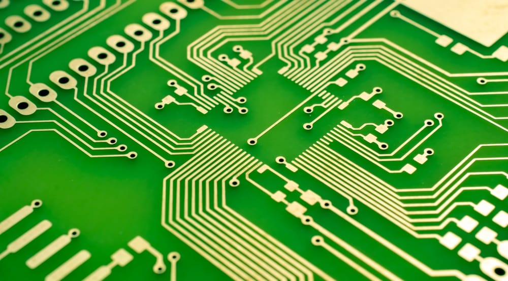
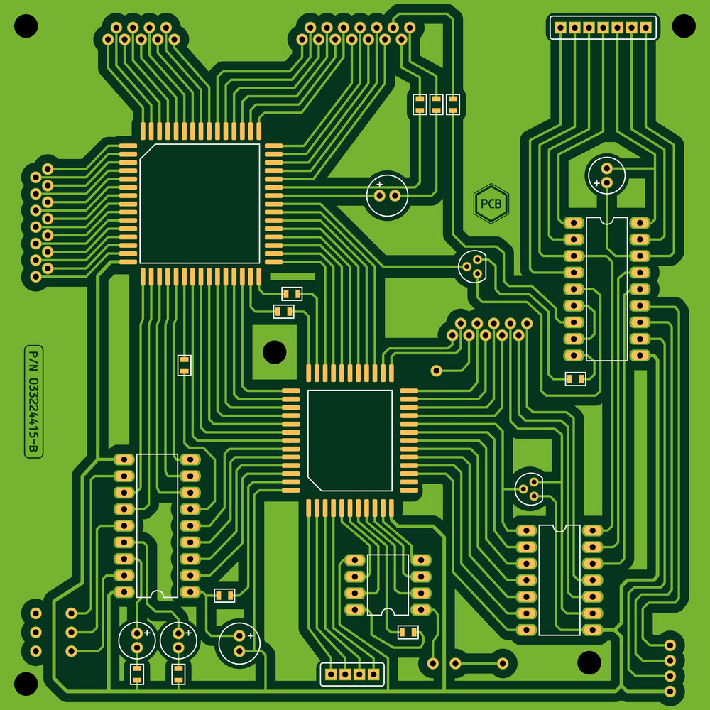
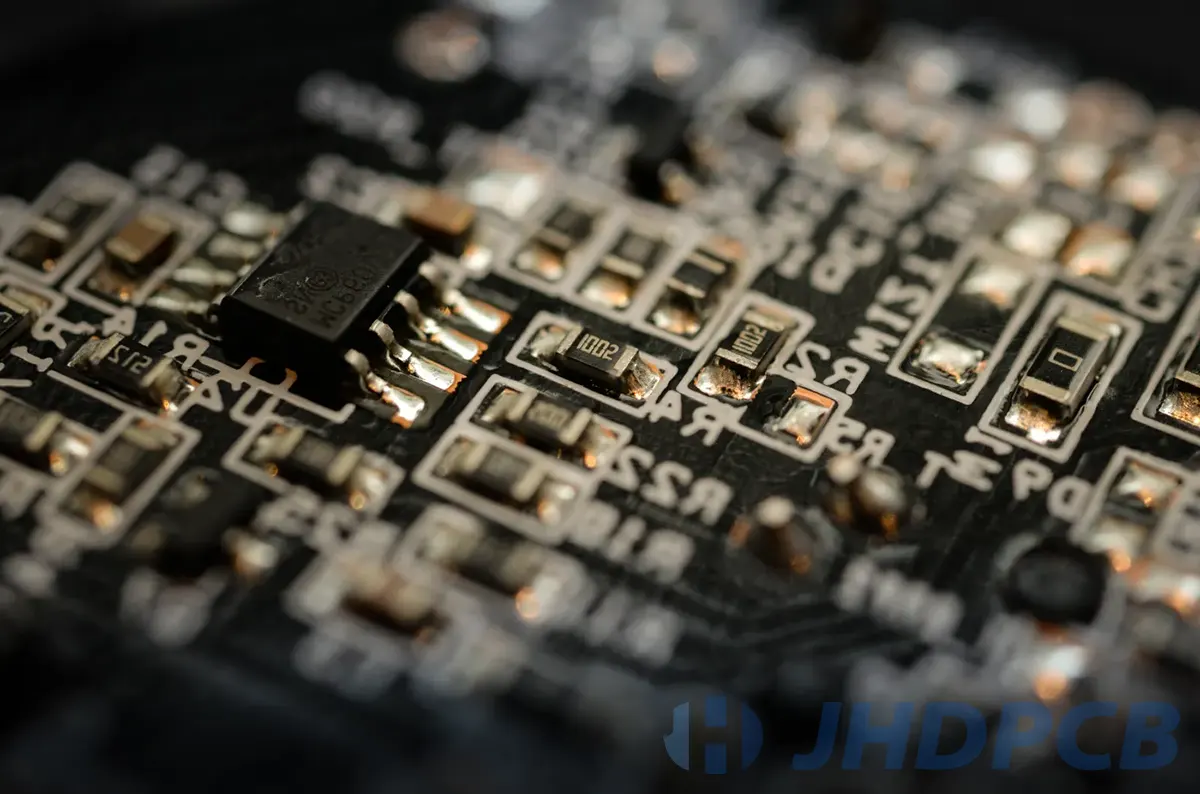
A PCB trace is a highly conductive track that is used to connect components on a printed circuit board. The traces are commonly made of copper and are fabricated during the etching process of a PCB. This article delves into the explanation of PCB trace, its vital components, and its significance to PCB design and fabrication.
Best Guide To PCB Traces: Width, Thickness And Design Fix Recommendations - Jhdpcb

A complete guide on PCB copper trace - PCBA Manufacturers
Kapton PCB- A Comprehensive Guide

Everything you want to know about PCB trace - IBE Electronics

Custom PCB-The Ultimate Guide

Ultimate Guide to PCB trace Printed Circuit Boards Canada by crimpcircuits - Issuu

How to pick the right Trace Width for PCB design? - PCB Design Tutorial - PCBway

A detailed guide to PCB layout design - IBE Electronics

Step-by-Step Guide to Repair PCB Trace - Fx PCB

All you need to know about PCB trace width calculator - IBE Electronics

PCB Design Guide to Via and Trace Currents and Temperatures: Brooks, Douglas, Adam, Johannes: 9781630818609: : Books
The Ultimate Guide To PCB Repair And Rework. - Jhdpcb
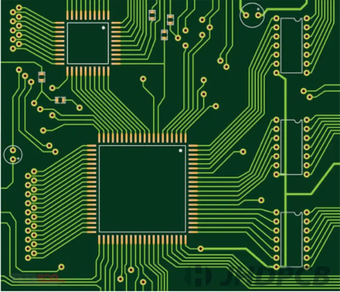
Best Guide To PCB Traces: Width, Thickness And Design Fix Recommendations - Jhdpcb
Circuit Trace – The Ultimate Guide
PCB Prices: What You Need to Know [Complete Guide]