PCB Via Filling Explained

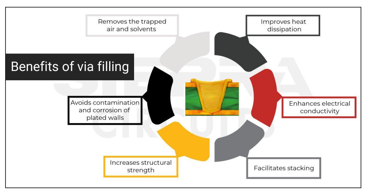
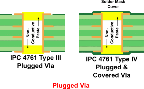
PCB Via Filling/Plugging is a process where the Via hole is filled with solder mask or resin to improve the reliability of the printed circuit board.

Plugging the Connection Gap: The Importance of Filled Vias in
Via Filling Techniques Designers Need to Know
Mistral Blog: Brief on High Density Interconnect PCB - HDI PCB
Technical Analysis Of Vippo Pcb/ Pofv Pcb

Via Hole Filling with resin
Via Filling Techniques Designers Need to Know
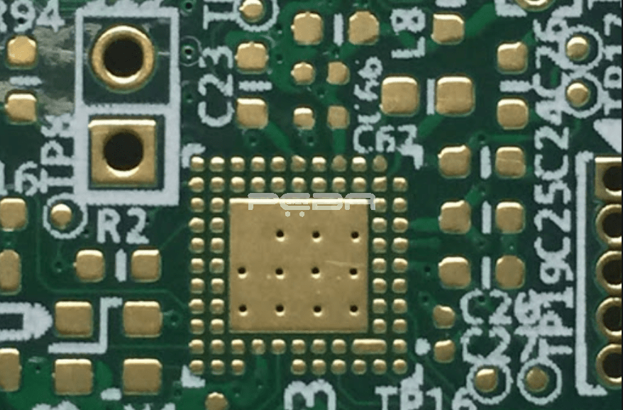
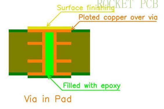
Everything About Via in Pad Technology
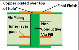
Non-Conductive Via Filling (NCVF) and Its Advantages
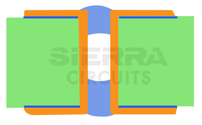
Pads, Vias And Holes
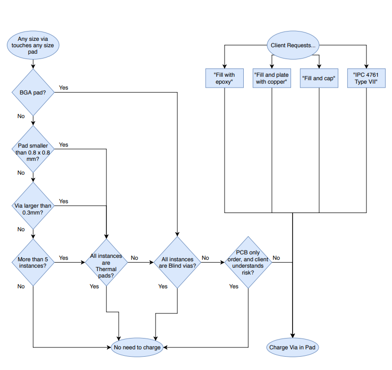
To Fill or Not to Fill Vias? - Rush PCB
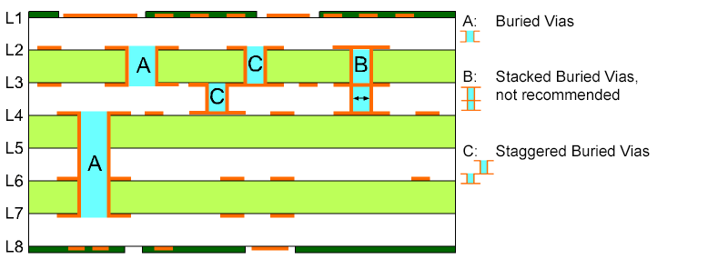
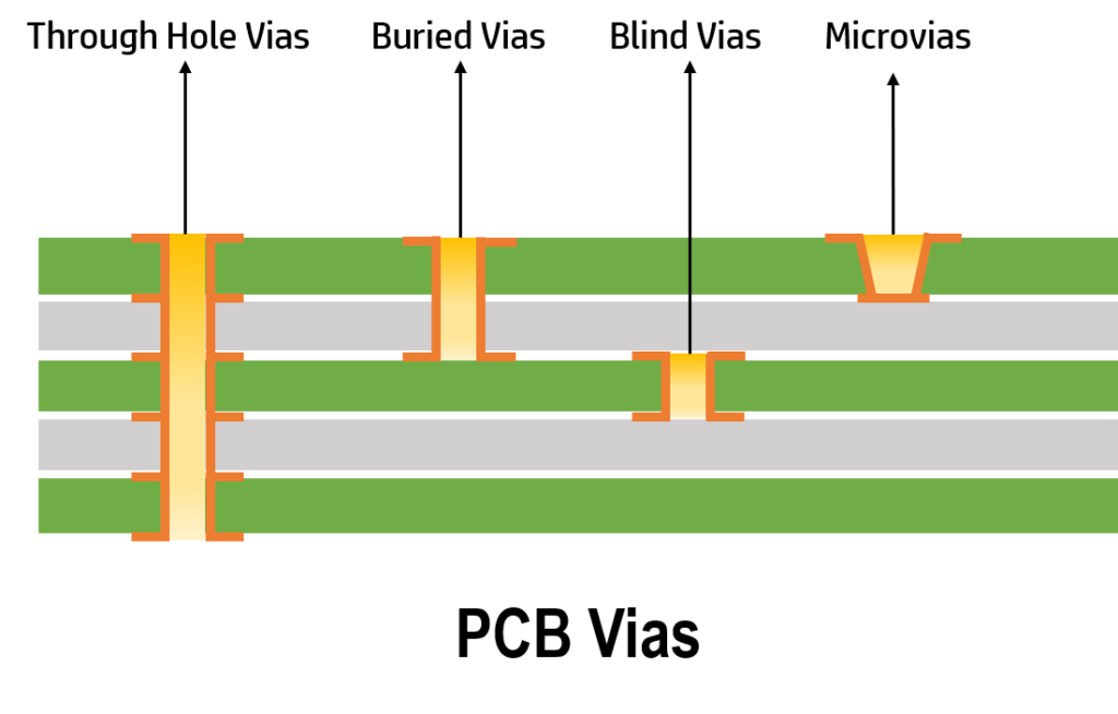
Blind Vias & Buried Vias - Multi Circuit Boards

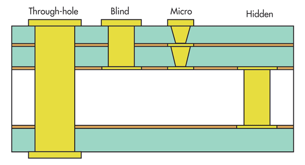
Via (electronics) - Wikipedia
PCB Vias - What Are Vias and Tenting Vias in PCB & Why Do You Need
PCB Vias - What Are Vias and Tenting Vias in PCB & Why Do You Need